As name suggests in this type of pcb a thin layer of conducting material like copper is applied to both top and bottom sides of the board.
Pcb board material name.
These are electrically connected by a hole through the board which is shown in figure.
However the needs of your board will invariably rely on various pcb material properties.
Components are generally soldered onto the pcb to both electrically connect and mechanically fasten them to it.
Alternately the acronym has also accounted for printed wiring boards and printed wiring cards which are essentially the same thing.
Like any other semiconductor package a qfn package functionality is to connect both physically and electrically silicon dies the asic to a printed circuit board pcb using surface mount technology.
Electronic components are then soldered onto this board making it a printed circuit board assembly.
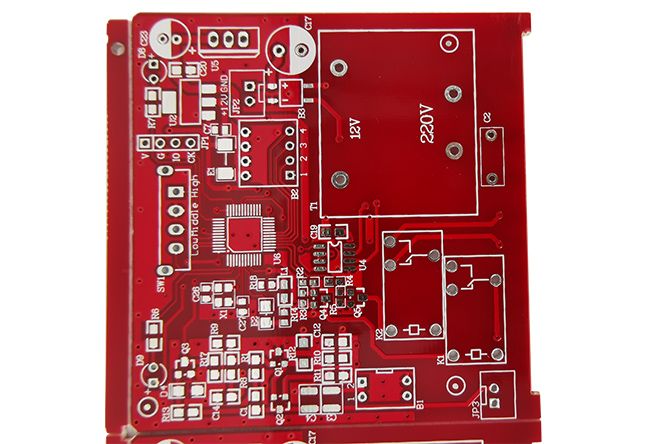
A printed circuit board pcb mechanically supports and electrically connects electrical or electronic components using conductive tracks pads and other features etched from one or more sheet layers of copper laminated onto and or between sheet layers of a non conductive substrate.
Printed circuit board is the most important part of electronics.
A pcb printed circuit board or pwb printed wiring board is a complex circuitry of copper tracks on a heat resistant material called pcb substrate.
You should choose the material of the pcb depending on the results that are expected.
Fr 4 is a common material for printed circuit boards pcbs.
Pcb materials can be classified according to their properties.
Electronic components are soldered on this circuit board to control flow of electricity in a preset matter for the electronic device to work in a manner that it was designed for.
A thin layer of copper foil is laminated to one or both sides of an fr 4 glass epoxy panel.
Uxcell double sided copper clad laminate pcb circuit board fr4 180x120mm 7 09x4 72 inch 1 5mm thickness diy prototyping pcb board name board 5pcs 4 8 out of 5 stars 18 14 39 14.
With all pcb material types the purpose is to conduct electricity and provide insulation between conducting layers of copper.
Due to the crucial role of these boards in everything from computers to calculators pc board material selection should be undertaken with care and.
The material is chosen according to the application the result needed environmental factors and any other constraints the pcb will face.
The different materials used for the pcb design and fabrication all offer a variety of advantages and disadvantages.
A printed circuit board pcb is a board made of different heat resistant insulating materials conductive copper tracks are printed or etched onto this con conductive base substrate.
These are commonly referred to as copperclad laminates.
When ordering a copper clad laminate board the fr 4 and copper thickness can both vary and so are specified separately.
Qfn is a lead frame based package which is also called csp chip scale package with the ability to view and contact leads after pcba.