The designer lays out a blueprint for the pcb that fulfills all the requirements as outlined.
Pcb design process steps ppt.
In our example we will use the led flasher circuit and design its pcb.
How do you design a pcb.
Step by step pcb designing tutorial.
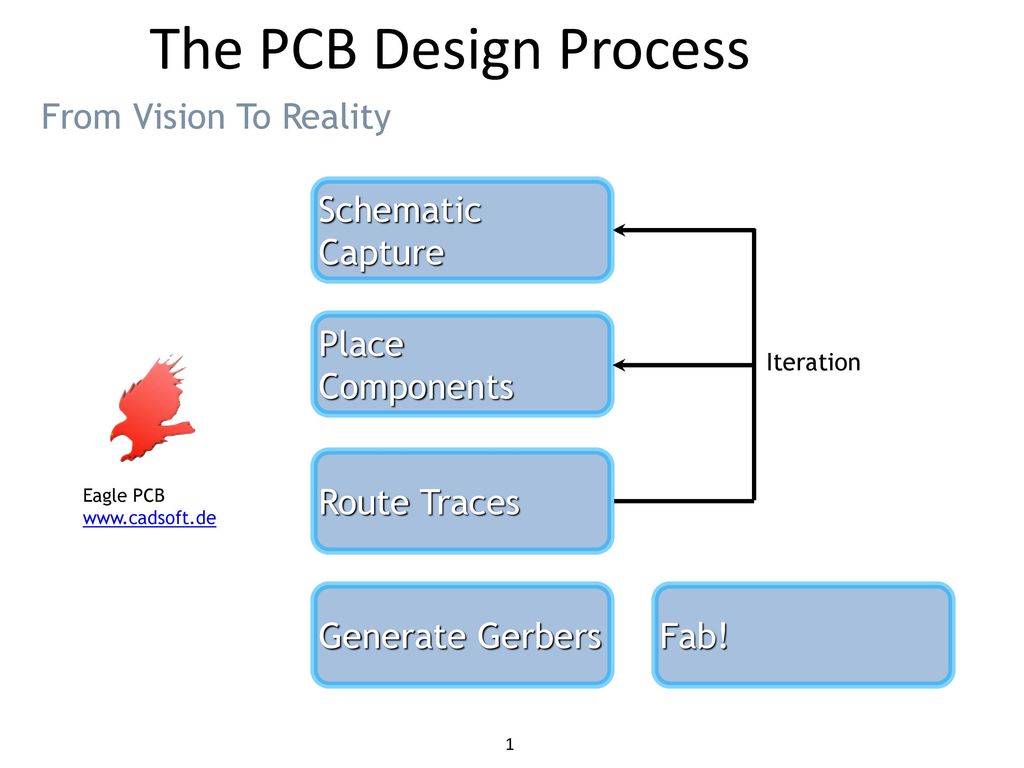
Follow my tradition schematic capture place components route traces gen gerbers fab.
The pcb layout and design has a major impact on the way in which a circuit work and therefore if the printed circuit board is designed in an effective way then the circuit will perform more reliably and within its specification.
How do you order a custom pcb.
Pcb manufacture and design always start with a plan.
Pcb design is an intricate process requiring careful consideration of a variety of factors and attention to the tiniest details.
And live to tell about it.
Overview what is a printed circuit board.
Knowing how to design a printed circuit board pcb is a key element of any electronic circuit design process.
Pcb design process 1.
All aspects of the pcb design undergo checks at this point.
Pcb design process free download as powerpoint presentation ppt pdf file pdf text file txt or view presentation slides online.
Pcb designing in ares capture proteus.
Iteration eagle pcb www cadsoft de generate gerbers schematic capture.
The steps of the pcb manufacturing process are as follows.
The beginning step of any pcb manufacture is of course the design.
What is a pcb.
Different pcb design software possibly calls for different gerber file generation steps they all encode comprehensive vital information including copper tracking layers drill drawing apertures component notations and other options.
How to design printed circuits boards.
P cad pcb user s guide i table of contents chapter 1 introduction to p cad pcb p cad pcb features 1.
Copper foil copper plating solder flow solder mask trace slots and cut outs 4.
What pcb is made of a basic pcb starts with a copper clad fiberglass material or thin copper sheets attached to either side of the board.
It consist of.
How to design a pcb step by step pictorial views with example pcb of led flasher circuit what is pcb printed circuit board.
Fabrication following are the basic steps of pcb design.